Printed Circuit Board (PCB)
Inspection Services
Today’s modern technology requires complex PCBs consisting of several layers and materials. Given the critical use and complexity of most PCBs, thorough PCB Inspection Services (with both a testing and inspection plan) are crucial to ensuring quality control at the earliest stages. One of the big advantages of PCB Qualification Testing is that you find out which conditions are acceptable versus nonconforming, which prevents you from needlessly scrapping quality boards and ensures that potential failures are caught early on and prior to full assembly.
Whether your printed circuit board testing plan includes external or internal inspection, the IPC-A-600 certified specialists at ORS are here to help!
We can assist you with the following:
Optical Inspection is a non-destructive method typically performed with the naked eye or under magnification. Externally observable conditions are those that are seen and evaluated on or from the exterior surface of the board. Typical characteristics observable from the surface are:
- Surface Imperfections – Burrs, nicks, scratches, gouges, cut fibers, weave exposure and voids.
- Subsurface Imperfections – Foreign inclusions, measling/crazing, delamination, pink ring and laminate voids.
- Imperfection in Conductive Pattern – Loss of adhesion, reduction of conductor width, or thickness due to nicks, pinholes, scratches, surface plating or coating anomalies.
- Hole Characteristics – Diameter, misregistration, foreign material, plating or coating anomalies, and scratches.
- Marking Anomalies – Location, size, readability and accuracy.
- Solder Mask Surface Coating Imperfections – Misregistration, blisters, bubbles, delamination, adhesion, physical damage and thickness.
- Dimensional Characteristics – PCB size and thickness, hole size and pattern accuracy, conductor width and spacing, registration and annular ring.
Internal Inspection requires micro-sectioning to detect any issues and evaluate observable conditions. In keeping with IPC-TM-650 Test Services, proper PCB microsection analysis provides a destructive means of inspecting several characteristics in the base material, plated through holes (PTHs), internal conductive copper pattern, treatments to the internal copper, and internal ground/power/thermal planes. Microsectioning is typically performed per IPC-TM-650 Test Method 2.1.1.
- Subsurface Imperfection in Printed Board Material – Delamination, blistering, cracks, ground plane clearance and layer-to-layer spacing.
- PTH Anomalies – Size, annular ring, nailheading, plating thickness, plating voids, nodules, cracks, resin smear, inadequate or excessive etchback, wicking, inner layer (post) separation and solder mask thickness.
- Internal Conductor Anomalies – Over or under etch, conductor cracks and voids, uneven or inadequate oxide treatment and foil thickness.
- Visual Observations – Made on cross-sections only.
Real Time PCB X-Ray Inspection is an ideal non-destructive technique for complex bare boards or densely populated assembled boards that contain mixed media such as through-hole devices, BGAs, CGAs or similar package types. X-Ray is typically performed per IPC-TM-650 Test Method 2.6.10. At the bare board level, ORS can inspect and evaluate whether:
- Innerlayer shift is within acceptable tolerances
- One or more inner layers have not been reversed
- Drilled holes are aligned with pads (to the extent that any break-out is within acceptable tolerances)
- The minimum distance between a drilled hold and a ground place clearance is within acceptable tolerances
- Solder joints of surface mount and through-hole devices are executed properly in assembled boards
Request a Demo or Follow-Up Call
Common Inspection Standards:
- IPC-A-600 – Acceptability of Printed Boards
- IPC-A-610 – Acceptability of Electronic Assemblies
- IPC-6012 – Qualification and Performance Specification for Rigid Printed Boards
- IPC-6013 – Qualification and Performance Specification for Flexible Printed Boards
- IPC-TM-650 – Test Methods Manual
- ECSS Q-ST-70-61C – High Reliability Assembly for Surface Mount and Through-Hole Connections
- ECSS-Q-ST-70-60C – Qualification and procurement of printed circuit boards
IPC Certificates:
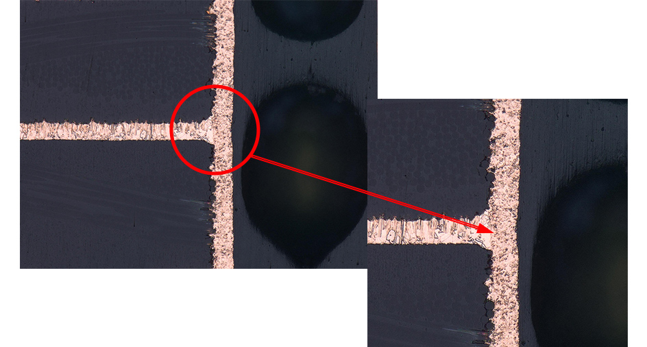
Per IPC-A-600K Nailheading
“No evidence exists that nail heading affects functionality. The presence of nail heading may be considered an indicator of process or design variation but is not cause for rejection”


