DESTRUCTIVE PHYSICAL ANALYSIS (DPA) TESTING FOR RESISTORS
ORS performs many different types of destructive and non-destructive tests on resistors to ensure that they meet the highest quality standards. Even the simplest parts can have problems!
A resistor is a two-terminal passive component that limits the flow of current in a circuit. Resistors are considered passive devices as they do not do anything active in a circuit, however, they are essential for building an active circuit.
There are two types of resistors: fixed and variable. Fixed resistors are designed such that the resistance value is not to be changed to adjust the circuit. The most commonly used fixed resistors are chip resistors. Variable resistors allow the user to change the resistance values depending on circuit need. Typical types of variable resistors are potentiometers and trimmers.
A variety of resistor constructions exist, some typical types are:
- Wirewound – Typically constructed by winding resistive wire around a core
- Foil – The resistive element is thin metal foil that is placed on a ceramic substrate
- Thick and thin film – Most common type of resistors, made with resistive layer on ceramic base
- Metal film – The resistive element is a combination of a ceramic material and a metal; the resistance value is adjusted to meets its target value by cutting a spiral pattern in the film
- Carbon film – A thin carbon film is deposited on the core and a spiral cut is made in the film to increase the resistivity
Although resistors appear to be simple, they require testing to ensure they meet quality standards. Typical non-destructive testing for resistors starts with external visual inspection. This test is the first step taken to identify overcoat, substrate and termination anomalies. Prohibited material inspection is also performed to ensure the termination materials meet the requirements or datasheet. Additionally, metal foil resistors (such as RNC90 style) and some resistor networks usually undergo terminal strength or pull testing to ensure internal welds are adequate.
The destructive phases of testing usually consist of a delid/decap of the outer housing and/or the resistor encapsulant. Variable resistors and resistor networks typically employ an outer housing that needs to be removed prior to inspection. This process is typically referred to as delidding. Chip resistors typically employ an overcoat that requires decapsulation to expose the resistive element for inspection. In addition to delid/decap, some resistors will also undergo a cross-section for internal inspection.
Contact us for information about Resistor testing
Test Methods:
For DPA, the following resistor types are covered within Mil-Std-1580 Revision C, Requirement 18:
- Variable wire wound
- Variable non-wire wound
- Resistor, metallized film
- Resistor, fixed metal foil (RNC90 style)
- Resistor, fixed, chip style
- Resistor networks
- Resistors, wire wound
- Resistors, fixed, wire wound – power and wire wound power, chassis-mounted
The following DLA performance specifications are available for resistors:
Mil-Prf-39015 – Variable Resistors
Mil-Prf-39035 – Variable Resistors, non-wire-wound
Mil-Prf-55182 & Mil-Prf-39017 – Resistor, metallized film
Mil-Prf-55182 – Resistor, fixed, metal-foil
Mil-Prf-55342 – Resistor, fixed, chip
Mil-Prf-83401 – Resistor networks
Mil-Prf-39005 – Resistor, wire-wound, accurate
Mil-Prf-39007 – Resistor, fixed, wire-wound, power
Common Failure Modes:
- Voltage or current surges (EOS) or ESD damage
- Sulfuration
- Resistive element burnout/deterioration
- Trim defects
- Electrode corrosion
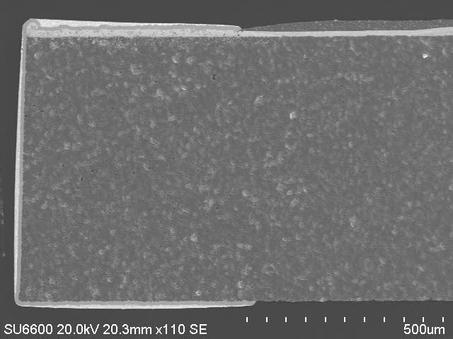
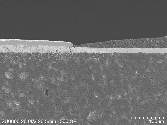
Figure 1.
Left image: SEM image showing the termination of a typical thick film chip resistor in cross-section.
Right image: SEM image showing the termination to overcoat interface in cross-section.
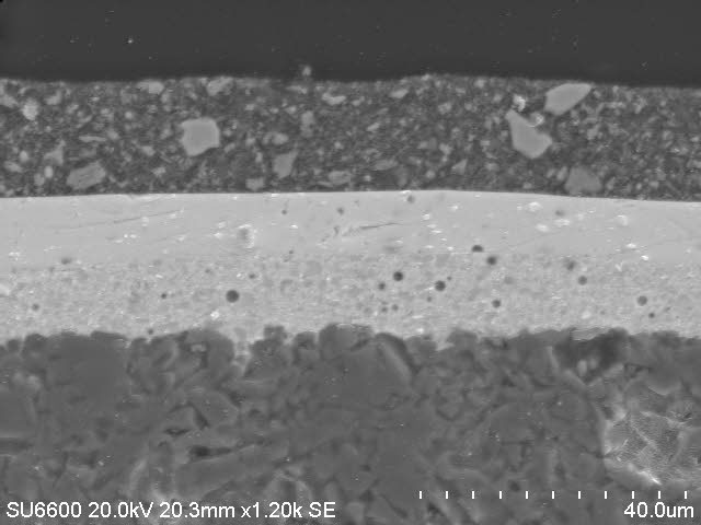
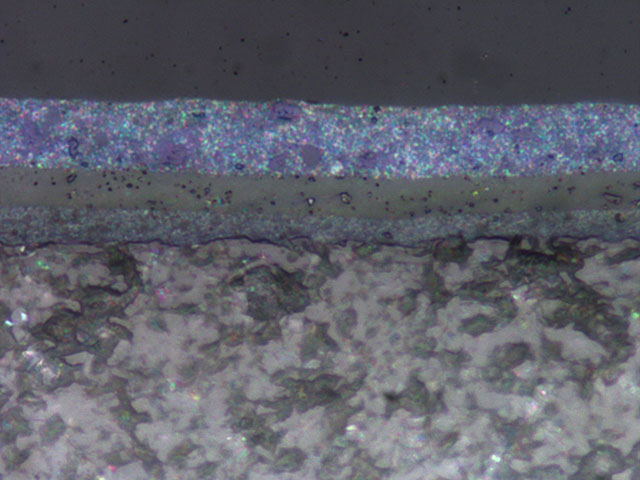
Figure 2.
Left image: SEM image showing the internal layers of a typical thick film chip resistor in cross-section.
Right image: Optical image of the internal layers seen on the left side.
Figure 3.
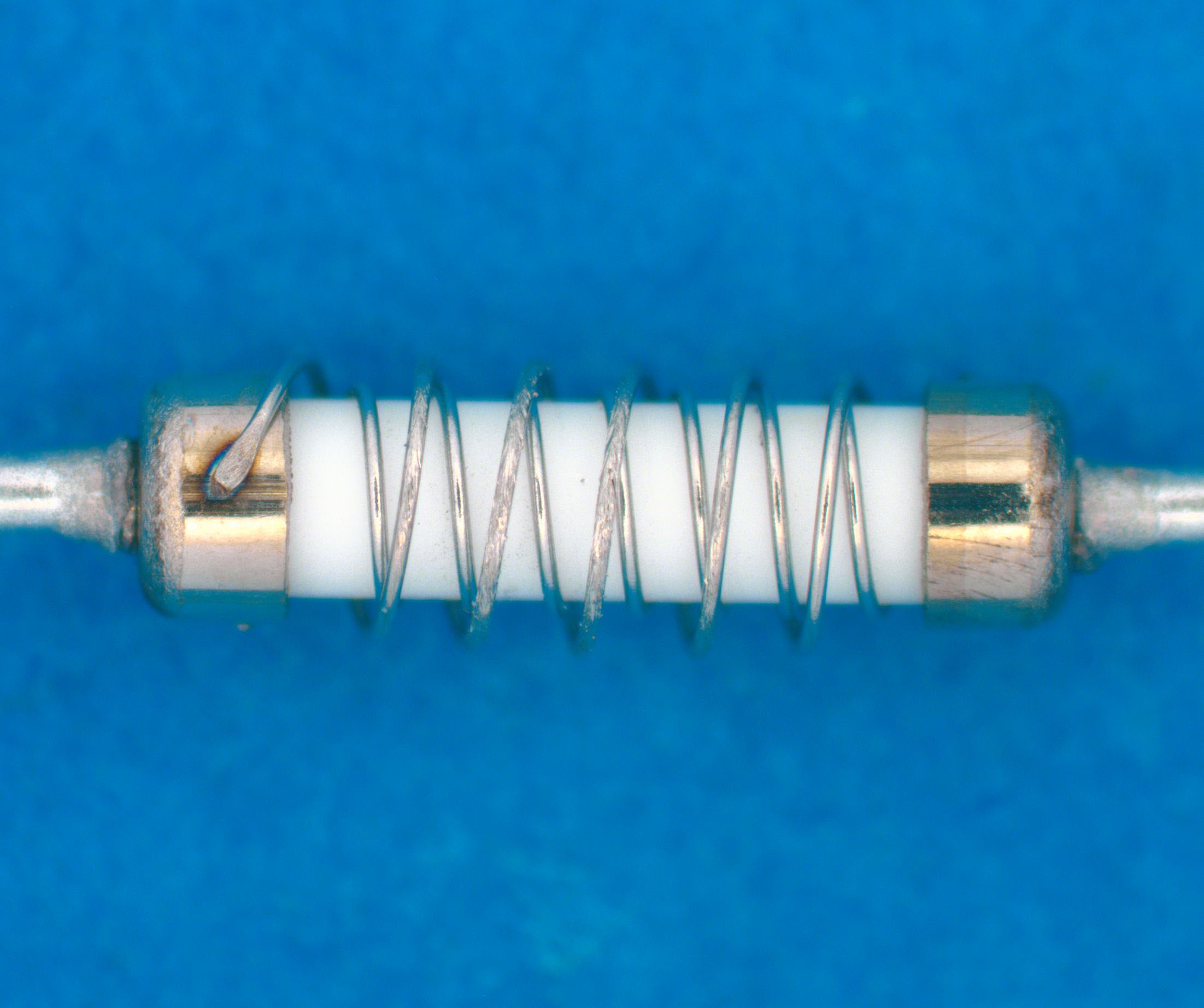
Left image: Optical image of a wirewound resistor after de-encapsulation.
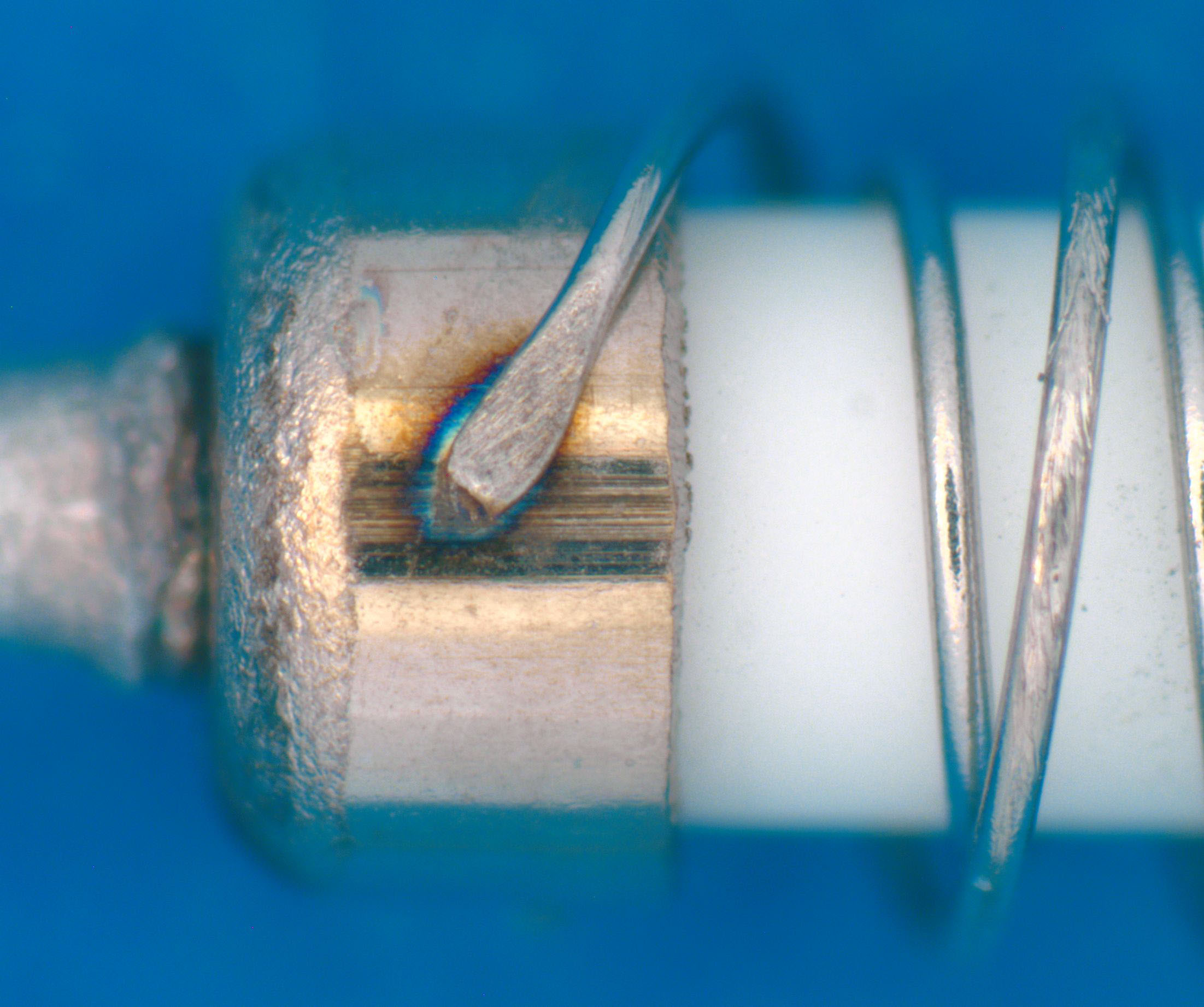
Right image: Optical image of a typical wire weld at the end cap.

