Destructive Physical Analysis (DPA) Testing for Transistors
Transistors are a fundamental component, critical to the function of nearly all electronic circuits. Due to their wide range of uses, discrete transistors can be packaged in many different ways to meet specific environmental, power and application requirements.
Typical transistor packages include hermetic sealed (ceramic bodied and metal TOs with lid-seam welds or solder seals), glass frit seals and a multitude of non-hermetic plastic encapsulations. All of these are prevalent in aerospace, military and automotive systems and are subject to qualification requirements under MIL-PRF-19500 and DPA MIL-STD-1580 and MIL-STD-750.
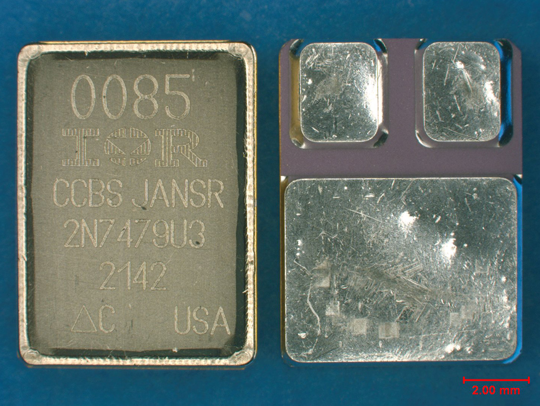
Hermetic SMD-0.5
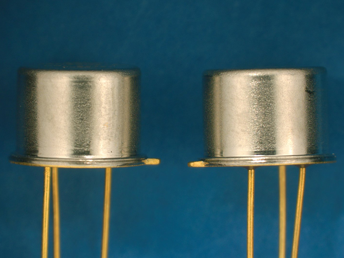
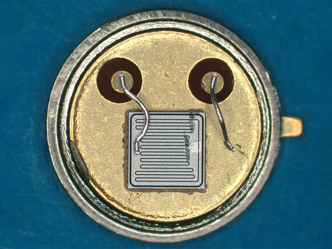
Hermetic TO
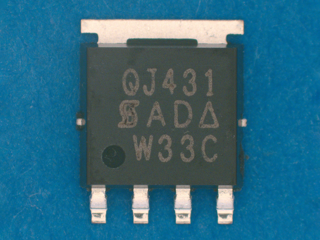
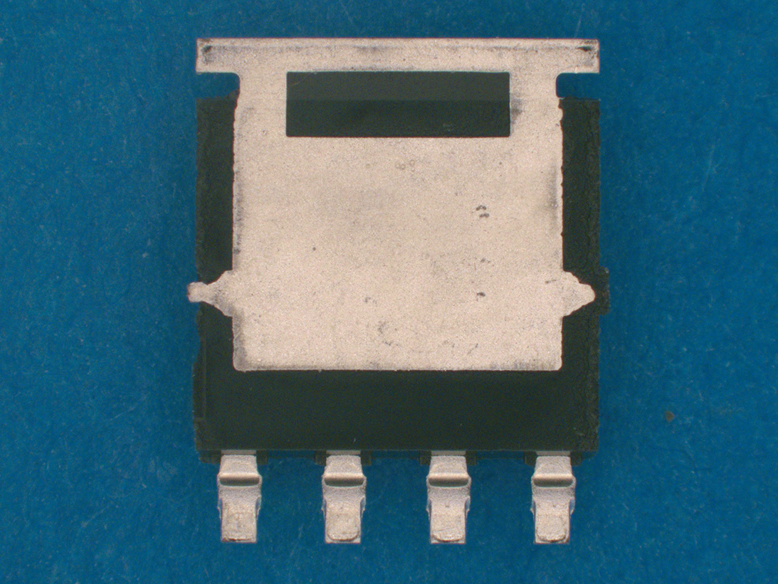
Plastic PowerPak SO-8L
ORS Offers FAST, Reliable Transistor DPA
Transistor device construction variations require specific test methods in DPA testing based on the Mil-PRF designs.
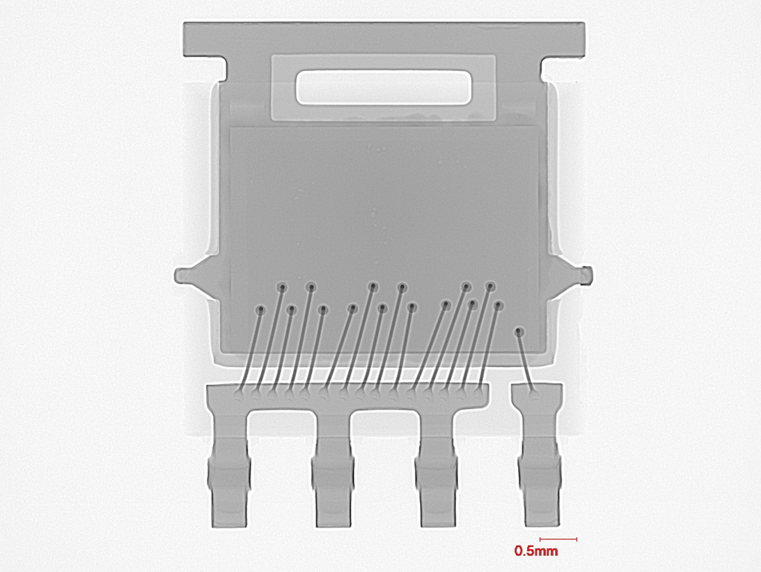
Transistors for aerospace applications must meet the requirements of MIL-STD-1580 Requirement 21 and require testing as outlined in Method 2102 MIL-STD-750. Additional test methods are also required based on design or construction. All designs require external visual inspection and X-ray radiography. Typically, PIND testing is required for hermetic packages.
Hermetic packages require additional MIL-STD-750 testing that includes hermeticity testing, Method 1071 and IGA Testing Method 1018. Bond strength and die shear testing Methods 2037 and 2017 along with overlay integrity and SEM metal inspection may be applicable as well.
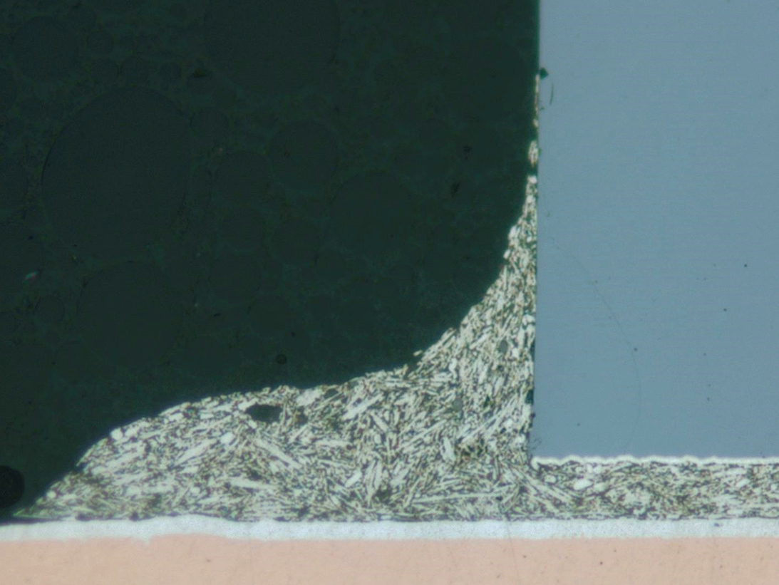
Plastic encapsulated devices may require acoustic microscopy, dye impregnation, cross-sectional inspection, bond pull (if applicable) and SEM metal test methods, depending upon metallization patterns.
Destructive Physical Analysis
ORS has over 45 years of experience performing comprehensive testing designed to identify anomalies that can lead to field failure.
ORS DPA techniques for transistors effectively reveal improper package markings, hermetic failures due to lid seal and glass feed-through, bond wire placement, intermetallic and lid clearance, die adhesion and metal-contact, step-thinning failures.
Contact us for information about transistors testing
Non-Destructive Test Methods
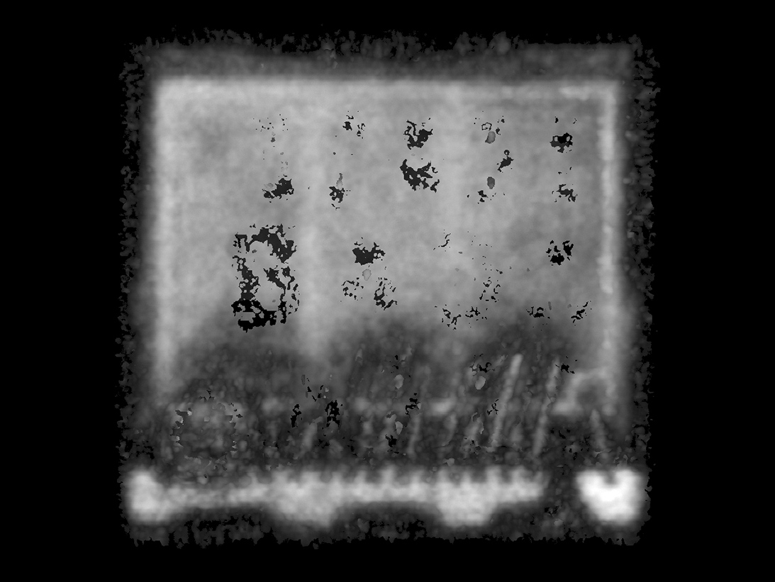
An important part of a transistor DPA are the initial non-destructive test methods that apply. These include external visual inspection with physical dimensions/configuration compliance, X-ray radiography, acoustic microscopy, hermeticity testing, particle-induced noise detection (PIND), prohibited-material analysis (PMA) by X-ray fluorescence elemental analysis (XRF) and Fourier transform infrared microscopy (FTIR).*
*FTIR is commonly included in baseline DPA or Construction Analysis (CA) type analyses to document functional groups detected in mold compounds and other organic features (i.e., die conformal coating and leadframe adhesives).
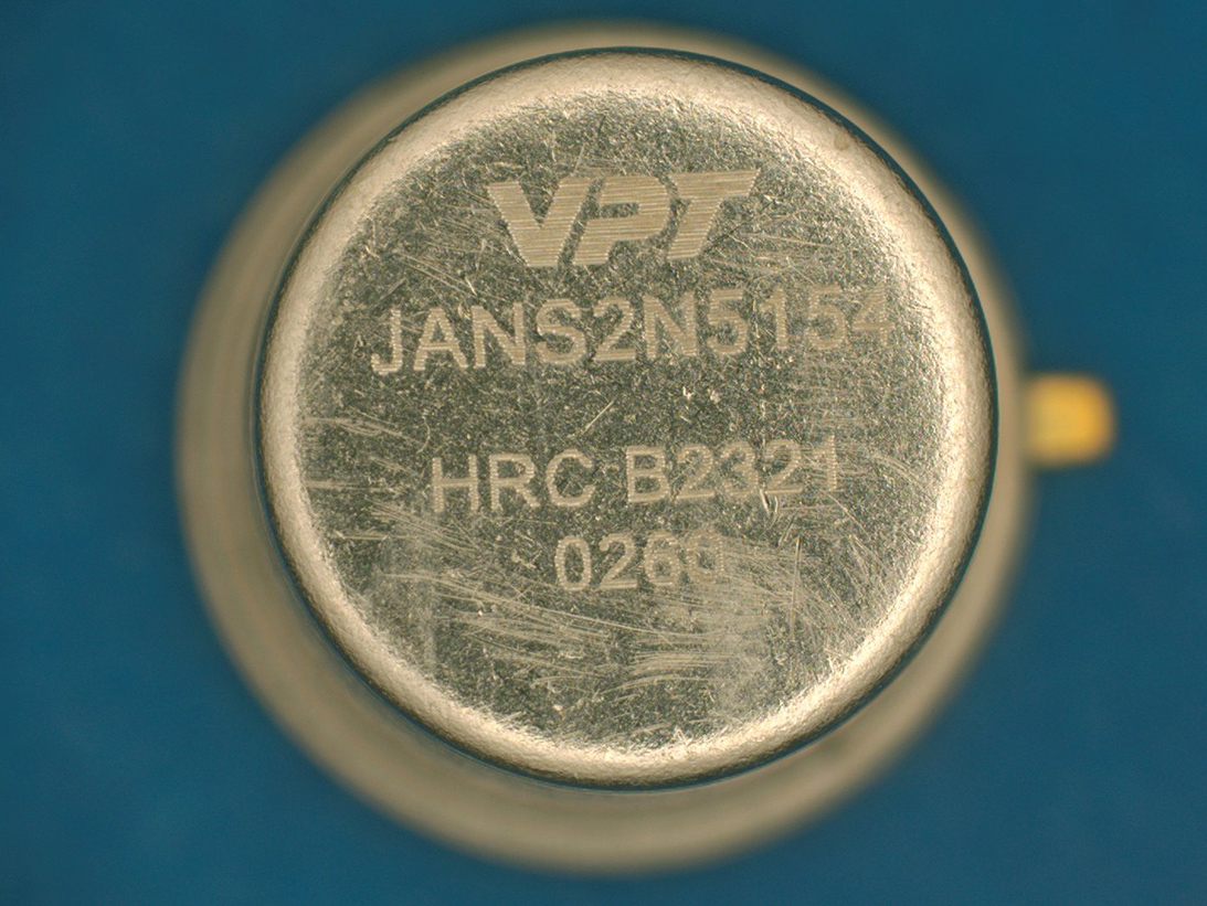
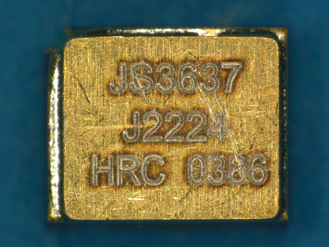
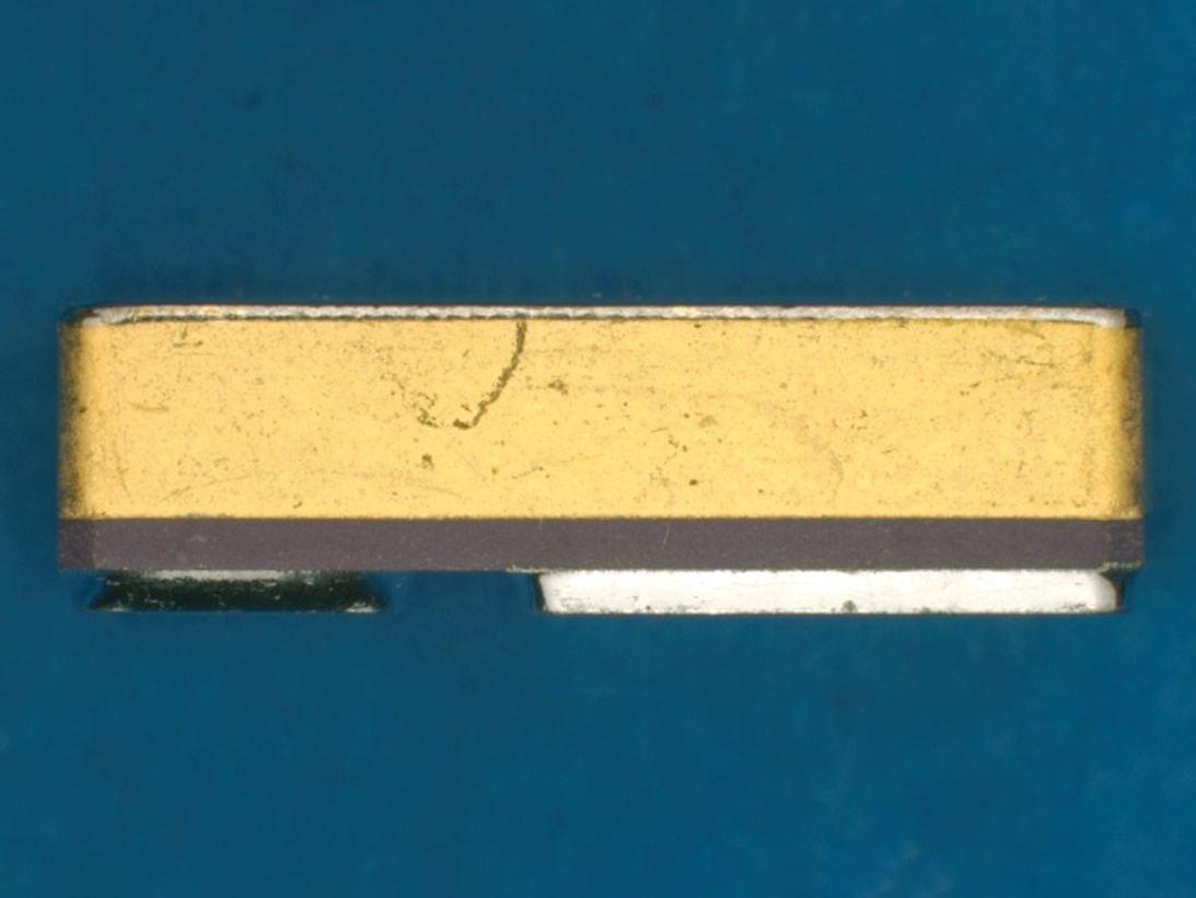
Device markings
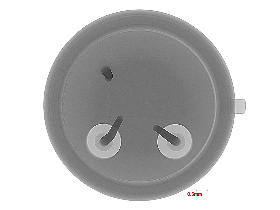
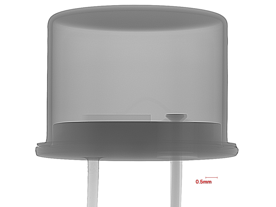
X-ray view of TO-can
X-ray Axial View
UB Solder Seal
Y-axis X-ray view
Z-axis X-ray view
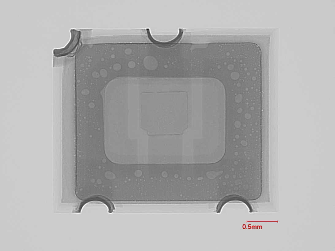
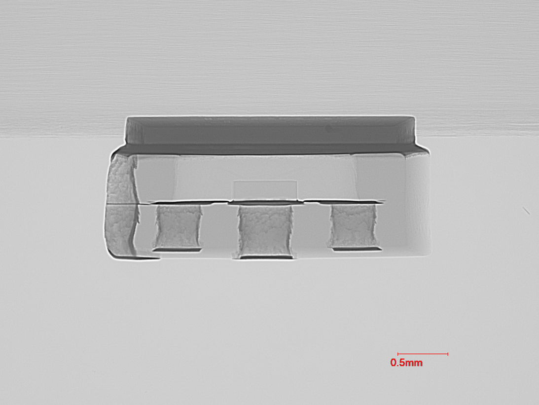
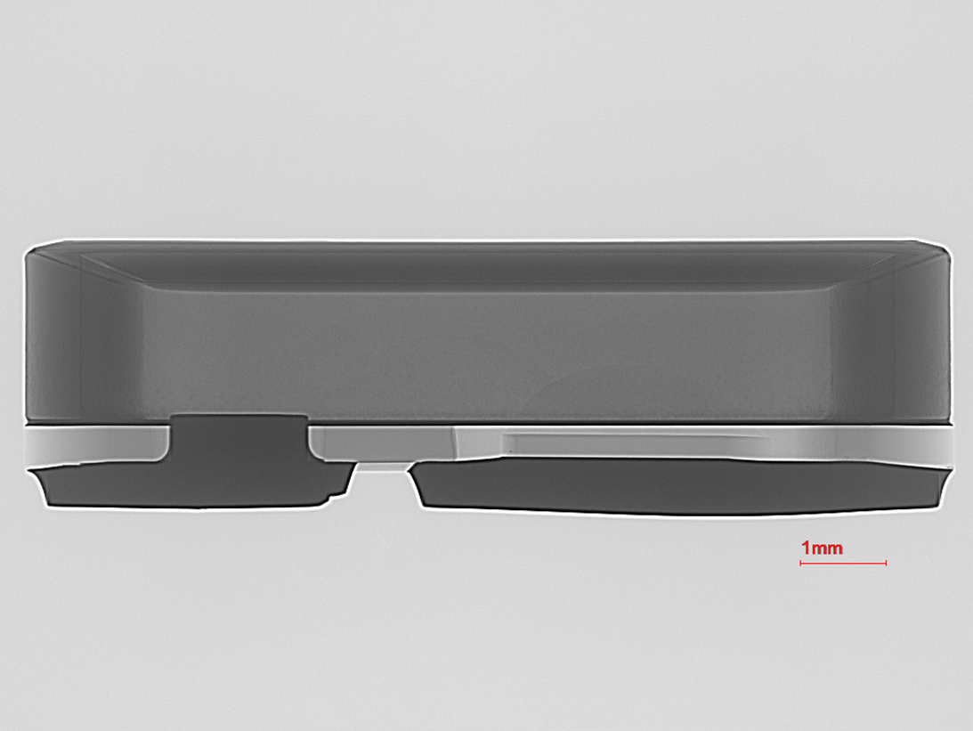
SEAM Weld SMD-0.5
X-axis X-ray of SMD-0.5
Extraneous Solder Ball
EMC
Y-axis X-ray image
Acoustic Image
Destructive Analysis Methods of Transistor Testing
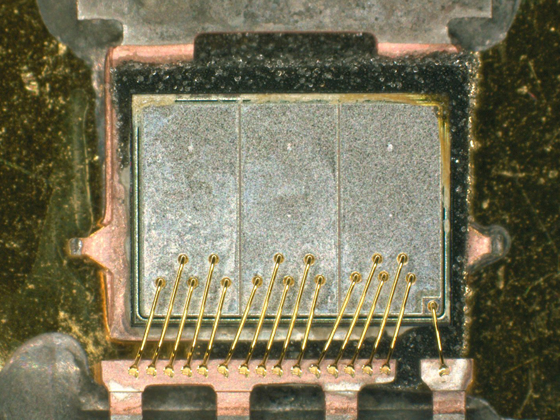
A complete DPA of a transistor could include destructive test methods such as IGA – internal gas analysis, internal visual inspection achieved by de-lidding/de-encapsulation or by cross-sectioning, bond strength testing and scribe and break methods. Transistor die with expanded metal require scanning electron metal inspection (SEM). SEM with energy dispersive X-ray (EDS) analysis may be utilized for internal prohibitive materials analysis testing.
Internal visual inspection De-lidded view of TO
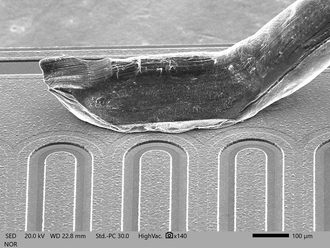
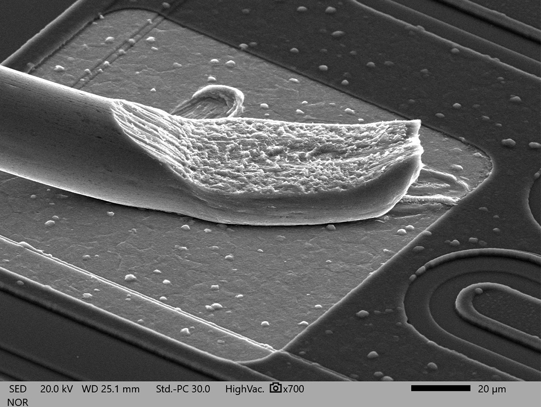
SEM image of wedg bond at die metal
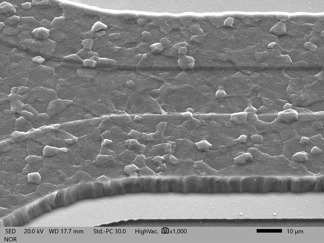
SEM image of metal step coverage
Internal cavity view UB Solder seal voids
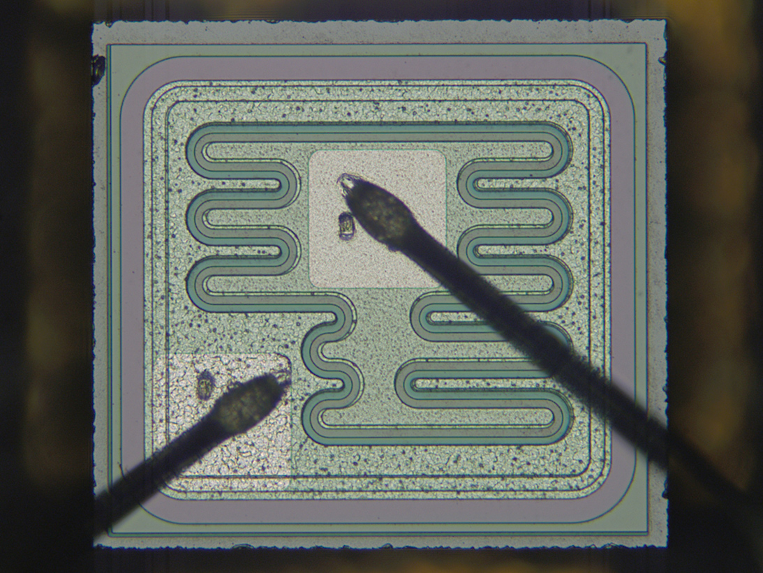
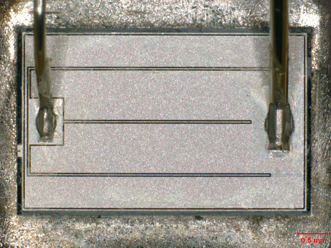
Overall die view
SEM of bond at die pad
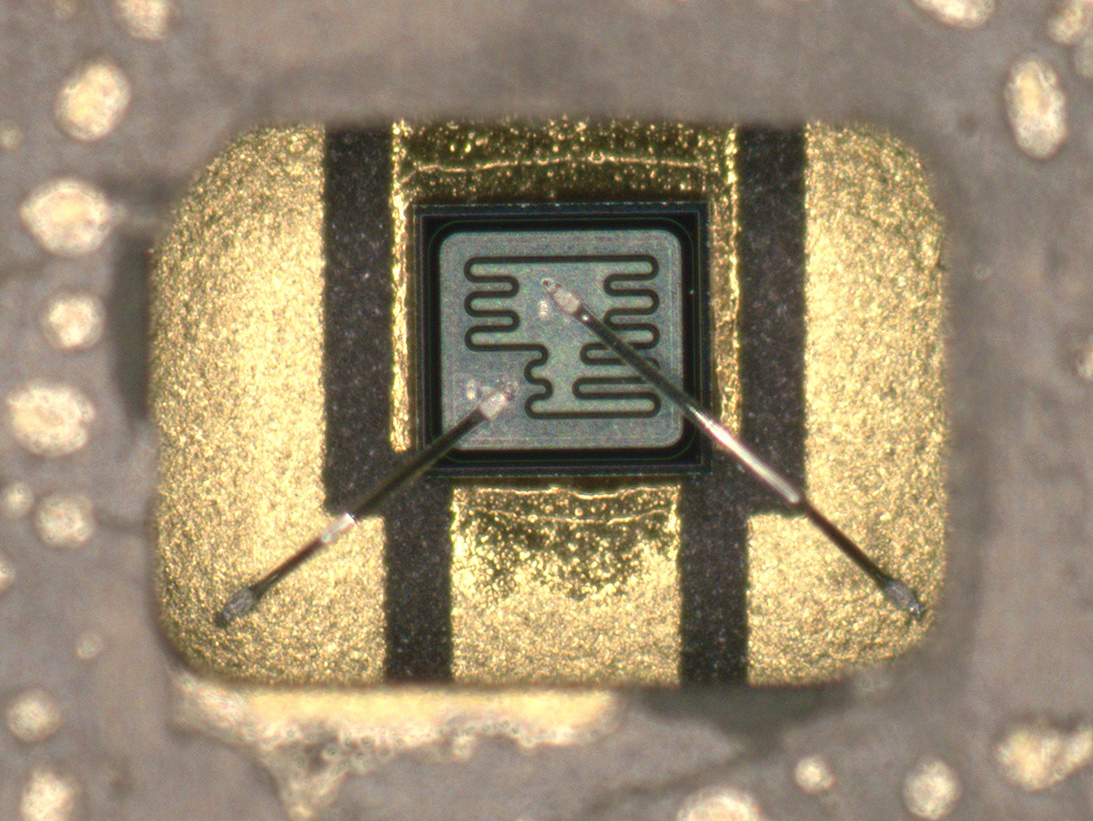
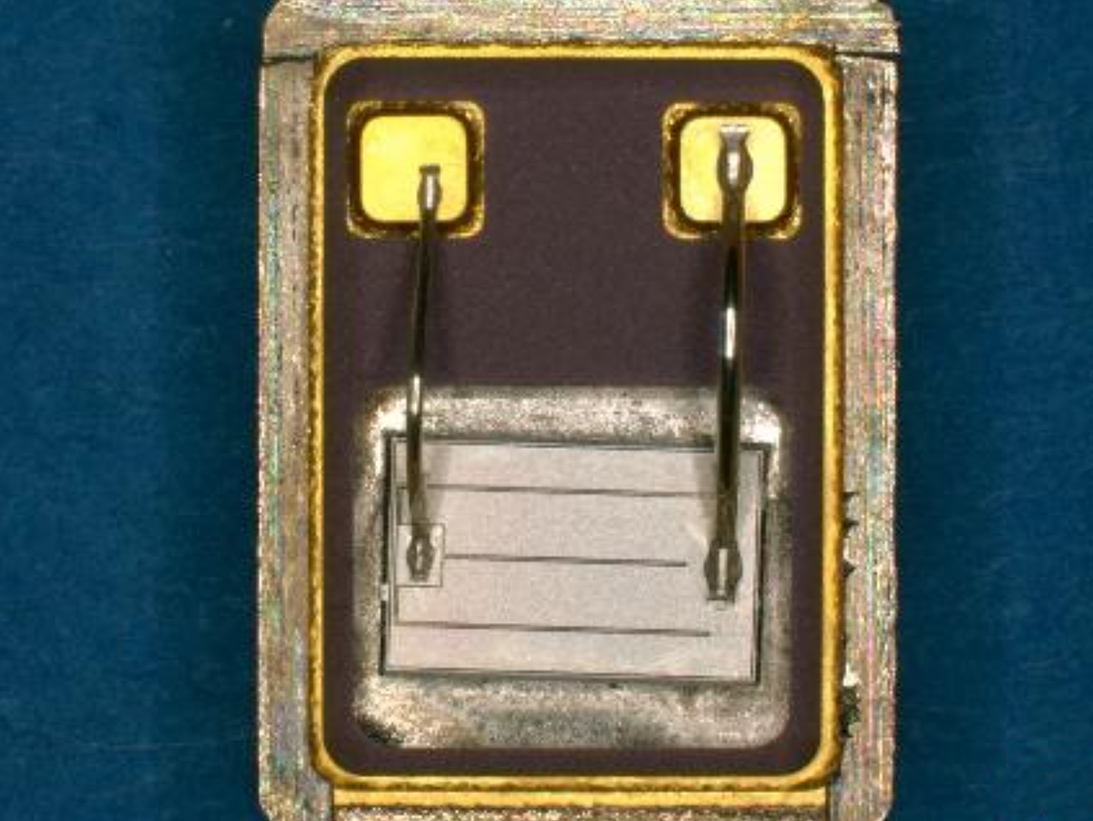
Internal view of SMD-0.5
FET Die
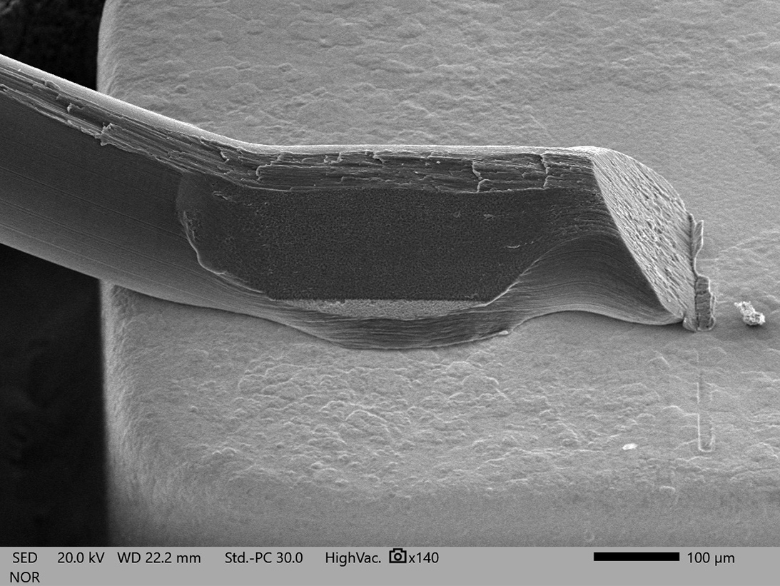
Wedge bond at post
PED De-encapsulated view
Cross-section view of bond
Cross-section view of die
Failure Modes of Transistors That Can Be Revealed by DPA:
Failure modes of Transistors will depend and vary on construction and by application
- Loss of Hermeticity/EMC delamination/moisture sensitivity/glass seals
- Wire bonding damage/ bimetallic intermetallic compounds
- Die scribing defects
- Pure tin at external surfaces and internal surface
- Undisclosed product changes
Applicable Industries:
- Space
- Aerospace
- Military Terrestrial
- Automotive/Commercial
- Mainframe Computers
Military Standards:
- MIL-PRF-19500
- MIL-STD-1580/Req 21
- MIL-STD-750 various Methods
Summary of Transistor Testing Methods
MIL-STD-1580 Requirement
MIL-STD-750 Test Methods
- External Visual – Method 2071
- Physical Dimensions
- Lead Finish Verification
- X-ray Radiography Method 2076
- Particle Induce Noise Detection Method 2052
- Acoustic Microscopy J-STD-035
- Dye Impregnation
- Internal Visual Inspection Method 2073
- De-encapsulation
- Cross-section
- Bond Strength Testing Method 2037
- Bond Shear Testing Method 2017
- SEM Metal Inspection Method 2077
- Prohibited Materials Analysis Req. 9

